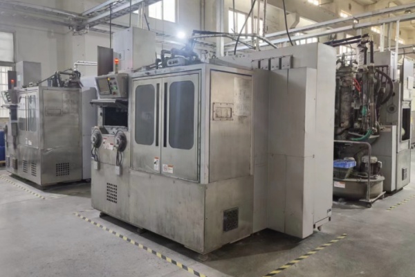
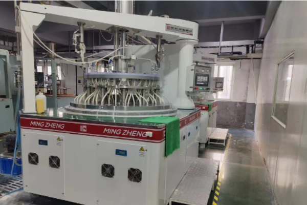
3. Rough Grinding (Lapping)
The raw slices carry deep saw marks and surface damage. During the lapping phase, double-sided grinding machines use large-particle silicon carbide or diamond slurry to rapidly remove the damaged layer. This brings the wafer very close to its target thickness and ensures parallel surfaces.
4. Chamfering (Edge Grinding)
Untreated wafers have razor-sharp, fragile edges. Chamfering utilizes precision profile grinding wheels to round off these edges. This crucial step prevents micro-chipping, structural fractures, and protects downstream processing equipment from scratches.
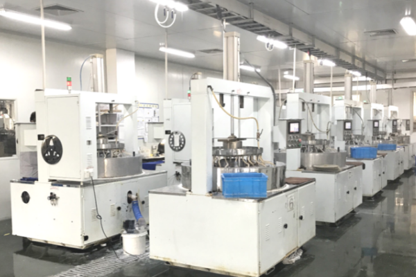
5. Fine Grinding
Building on the lapping process, fine grinding uses micro-abrasives to dramatically improve the surface roughness (Ra value). This creates a highly uniform, smooth texture that prepares the wafer for the ultimate finishing step.
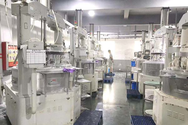
6. Polishing (CMP)
This is the magic step that determines the final surface quality of the sapphire substrate. Using Chemical Mechanical Polishing (CMP) technology, the wafers are polished with a nanoscale silica slurry and specialized polishing pads. This combination of physical friction and chemical reaction removes the last microscopic imperfections, yielding a pristine, Epi-ready mirror finish.
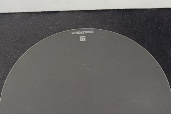
7. Laser Marking
For full product traceability, high-precision laser marking machines engrave a unique QR code or alphanumeric serial number near the wafer’s edge. The laser parameters are strictly controlled to ensure clear marking without generating micro-particle contamination.
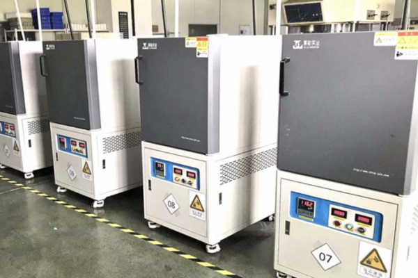
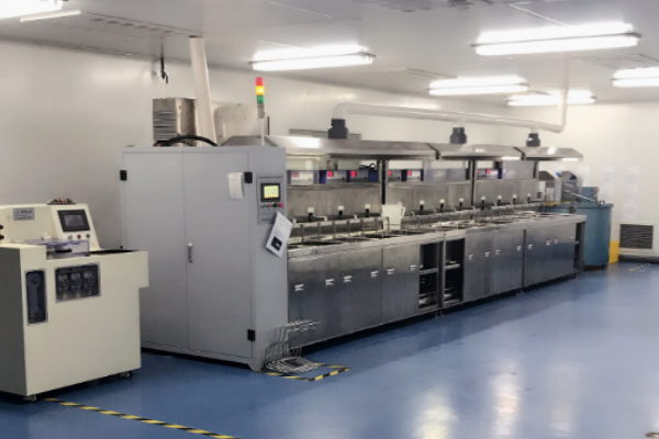
8. Cleaning
After enduring intense grinding and polishing, the wafers must be completely purged of slurry residue, organics, and metallic ions. They undergo a rigorous multi-tank ultrasonic cleaning process using specialized chemicals (such as RCA cleaning) and ultra-pure water to achieve absolute cleanliness.
9. Inspection & Metrology
Cleaned wafers are moved into a strict cleanroom environment for final quality control. Using automated optical inspection (AOI) and advanced metrology tools, engineers measure Total Thickness Variation (TTV), BOW, WARP, and scan for microscopic surface defects. Only flawless pieces pass as certified substrates or optical windows.
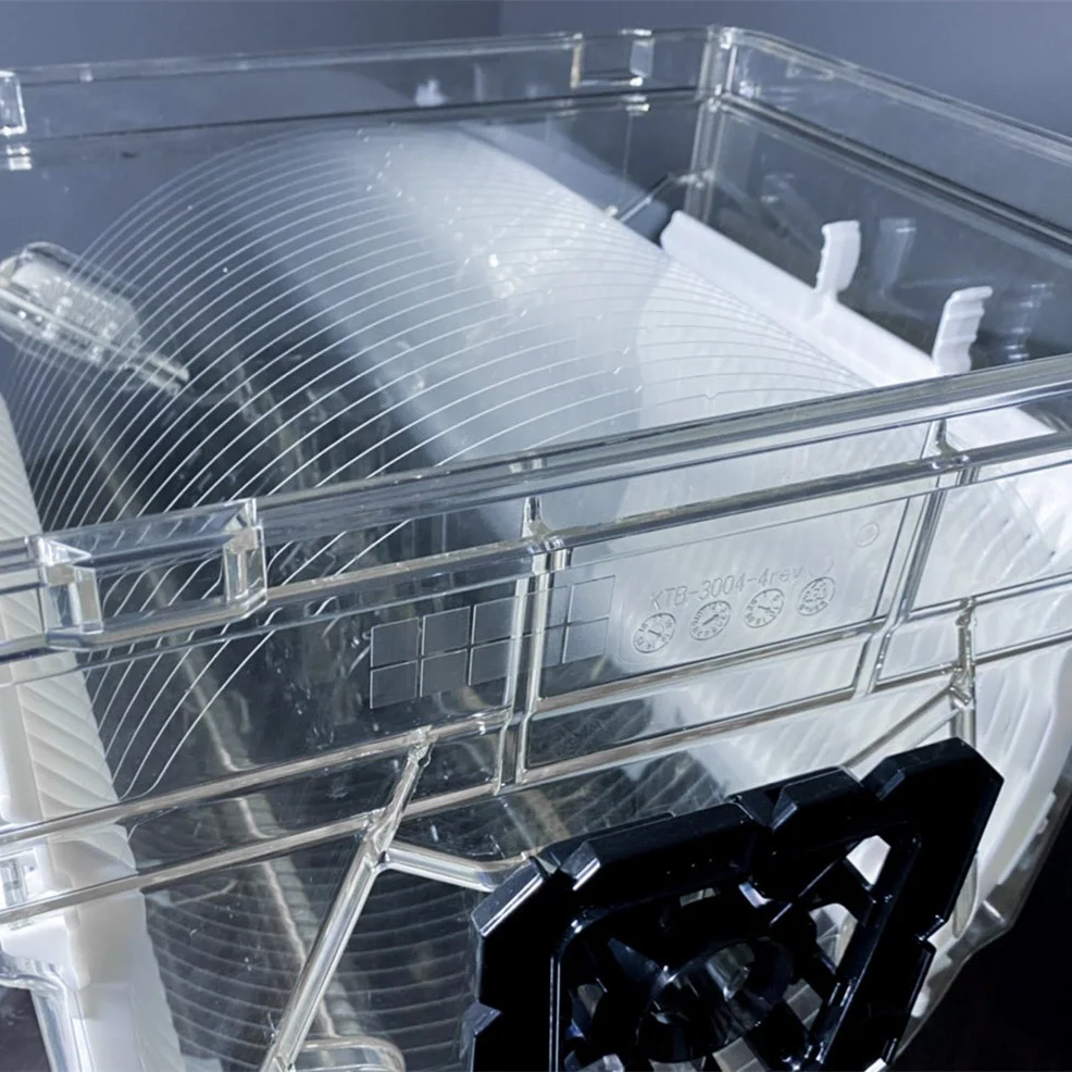
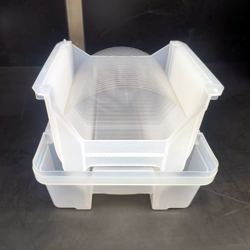
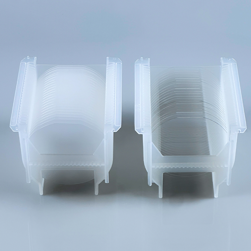
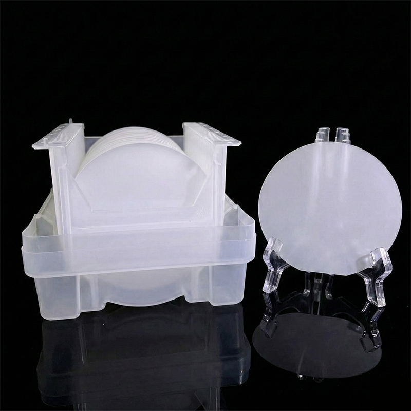
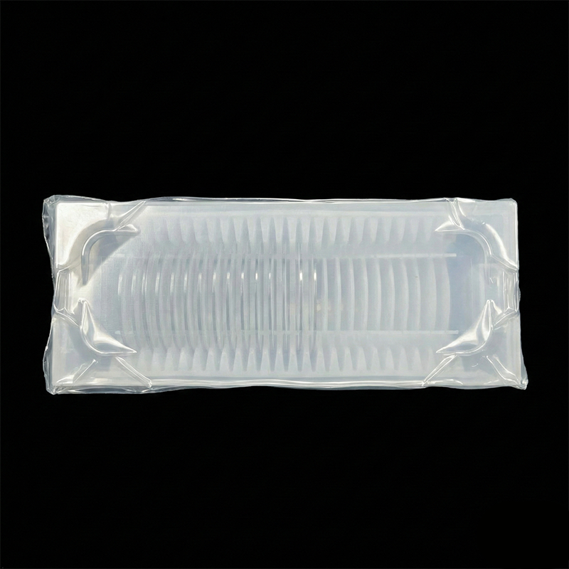
10. Packaging
In a Class 100 (or higher) ultra-clean environment, the finished wafers are loaded into specialized cassettes or coin boxes. They are vacuum-sealed and filled with inert gas to prevent static buildup and particle contamination, guaranteeing they arrive at the customer’s facility in perfect, ready-to-use condition.
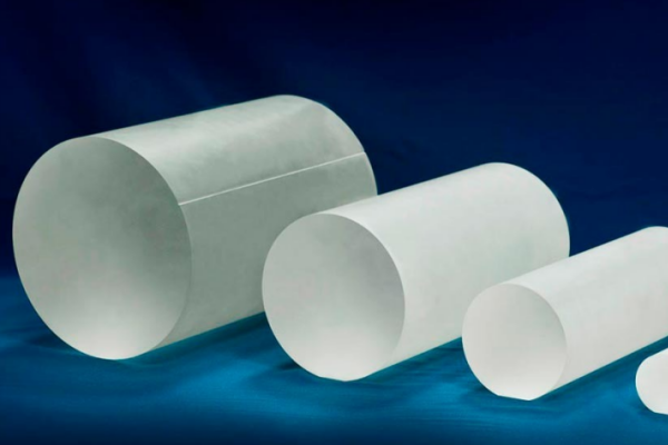
Our Premium Sapphire Wafer & Window Solutions
Backed by cutting-edge processing equipment and rigorous quality control, we provide a comprehensive range of sapphire solutions for the global optoelectronics, aerospace, and semiconductor industries. Our core product portfolio includes:
Epi-Ready Sapphire Substrates: High-flatness 2-inch, 4-inch, 6-inch, and 8-inch wafers optimized for epitaxial growth in LED and micro-LED displays.
Patterned Sapphire Substrates (PSS): Designed to significantly enhance light extraction efficiency and improve epitaxial layer quality.
Premium Sapphire Windows: High-transmission, extreme-pressure resistant optical windows for aerospace, deep-sea sensors, and harsh industrial environments.
Consumer Electronics & Wearables: Scratch-resistant sapphire glass for smartwatch screens, camera lens covers, and mobile device displays.
Special Orientation Wafers: Custom A-plane, R-plane, and M-plane substrates tailored for Silicon on Sapphire (SOS) RF applications and specialized microelectronics.