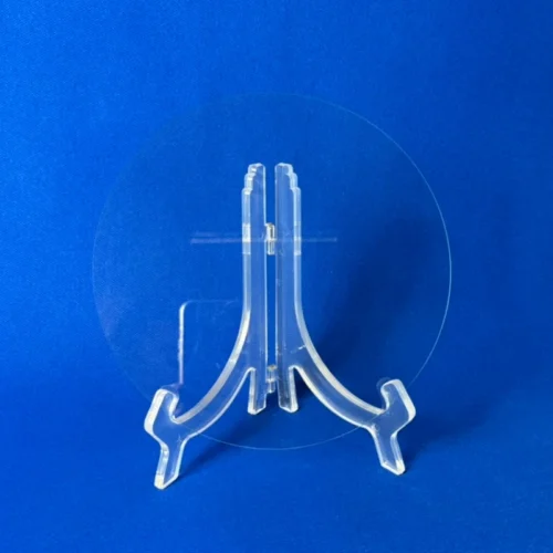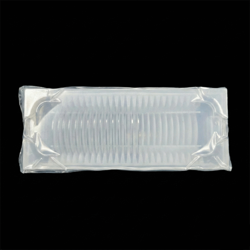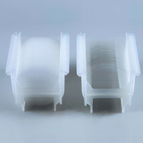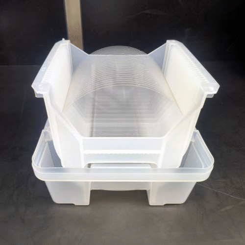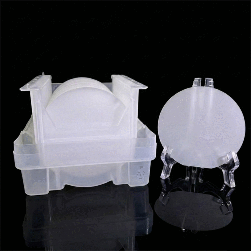
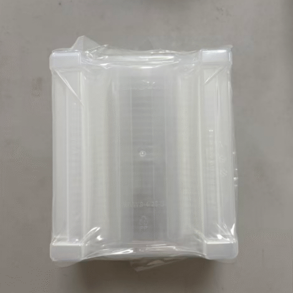
100mm Double Side Polished Sapphire Substrate
Accelerate your optoelectronics fabrication with our high-grade 100mm (4-inch) sapphire carrier substrates. Recognized as a staple material across global semiconductor markets, this specific DSP configuration is heavily relied upon by top-tier fabs worldwide for handling ultra-thin layers during mass transfer, temporary bonding, and back-end processing.
Core Material Specifications
To eliminate variations in your production line, every substrate is manufactured to rigorous dimensional and crystallographic tolerances.
-
Wafer Diameter: 100 ± 0.2 mm
-
Thickness: 650 ± 15 µm
-
Orientation: C-Plane ± 0.3°
-
Primary Flat Length: 30 ± 1 mm
-
Polishing: Double Side Polished (DSP)
-
Roughness (Ra): < 0.3 nm
Global Supply & Surface Preparation
Because this 650µm specification is highly sought after by global display and semiconductor manufacturers, we maintain a massive, ready-to-ship inventory in our facilities. This allows us to offer exceptionally short lead times for both prototyping and high-volume production orders worldwide.
To match your cleanroom requirements, we provide tailored surface preparation:
-
Standard Processing: Industrial ultrasonic cleaning.
-
Advanced Processing: Semiconductor-grade CRC-100 cleaning is available, delivering an ultra-clean, particle-controlled surface optimal for direct wafer bonding.