We use cookies to enhance your browsing experience, serve personalized ads or content, and analyze our traffic. By clicking "Accept All", you consent to our use of cookies.
How Surface Defects Affect GaN Epitaxy on Sapphire
As an epitaxy engineer working with LED or high-electron-mobility transistor (HEMT) production, you know that achieving a flawless Gallium Nitride (GaN) layer is an unforgiving process. When your GaN epitaxy yield inexplicably drops, the root cause is rarely the MOCVD reactor itself. More often than not, the silent killer is lurking on the surface of your sapphire substrate, specifically originating from the Chemical Mechanical Polishing (CMP) stage.
Because GaN and sapphire already have a natural lattice mismatch, the substrate’s surface must be atomically flat. Even nanometer-scale anomalies can nucleate massive dislocation arrays in the epitaxial layer.
In this guide, we will break down the critical CMP-induced surface defects that ruin epitaxy runs and explain the mechanics behind them.
The Micro-Roughness Disaster: Orange Peel and Waviness
To achieve epi-ready atomic flatness, the CMP process relies on a delicate $1:1$ balance between chemical softening and mechanical removal. When this balance fails, macro-scale roughness emerges.
Orange Peel & Waviness
The Mechanics: Orange peel and waviness occur when the chemical etching component of the CMP slurry is too aggressive compared to the mechanical action of the polishing pad. This is frequently triggered by an inappropriate pH level in the slurry or non-uniform rotation of the polishing plate.
Impact on Epitaxy: Instead of providing a uniform planar foundation, the chemical slurry preferentially attacks certain crystallographic orientations. This uneven chemical thinning creates a surface resembling water ripples or citrus skin. When GaN is deposited over these undulating topographies, it creates highly uneven strain fields, leading to cracked epi-layers and drastically reduced internal quantum efficiency (IQE) in LEDs.
The Hidden Killers: Polishing Haze and Pits
Sometimes a sapphire wafer appears perfectly flat to the naked eye but fails miserably in the epi-reactor. This is often due to residual mechanical damage from earlier, rougher processing steps (like lapping) that the final CMP stage failed to erase.
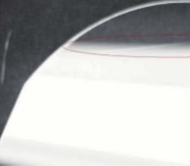
Polishing Haze
The Mechanics: CMP polishing haze is a macroscopic, smoke-like defect caused by the diffuse reflection of external light. It is the direct result of incomplete polishing. While the surface may feel smooth, it is actually covered in millions of sub-micron scratches.
Impact on Epitaxy: Haze indicates a severe lack of atomic-level order. Attempting to grow GaN on a hazy substrate is like trying to build a house on gravel; the nucleation layer will form irregularly, leading to unacceptable levels of threading dislocations.
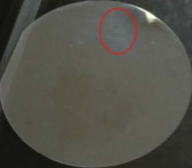
Dimples and Pits (The SSD Problem)
The Mechanics: Before CMP, sapphire wafers undergo aggressive mechanical grinding, which leaves behind sapphire SSD (sub-surface damage)—a microscopic network of stress and fractures just below the surface. If the CMP process doesn’t polish deep enough to remove this SSD layer, the chemicals will seep into these micro-cracks. Through a process called preferential etching, the slurry aggressively hollows out these stress points, turning invisible micro-cracks into visible dimples and pits.
Impact on Epitaxy: Each pit acts as a void that disrupts the continuous flow of reactant gases during MOCVD. These localized depressions force the epitaxial layers to grow at skewed angles, eventually resulting in fatal electrical shorts or dark spots in the final device.
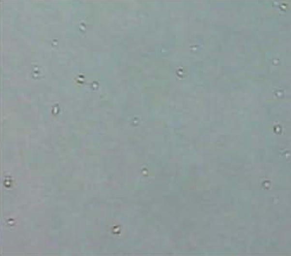
Fatal Contamination: Surface Contaminants
Even if you achieve a perfectly polished, zero-haze surface, improper handling in the final meters of the race can ruin the entire wafer.
Slurry Residue and Mishandling
The Mechanics: Sapphire surface contaminants include residual polishing slurry, dust, and human fingerprints (salts and oils). They occur due to incomplete ultrasonic cleaning or improper cleanroom inspection handling.
Impact on Epitaxy: MOCVD reactors operate at extreme temperatures (often exceeding 1000°C). At these temperatures, surface contaminants do not simply burn off; they bake directly into the crystal lattice. A microscopic drop of dried polishing slurry will act as a foreign mask, blocking GaN nucleation in that specific area and creating a massive void in the epi-structure.
Securing Your Yield with Epi-Ready Sapphire
Epitaxy is an expensive and time-consuming process. You cannot afford to use substrates that harbor hidden SSD, polishing haze, or chemical imbalances.
Demand better from your substrates.
Our Epi-Ready C-plane sapphire wafers are processed using a highly optimized CMP balance and multi-stage ultrasonic deionized (DI) water cleaning protocols. Every batch is rigorously inspected to ensure a strictly zero-haze, contaminant-free surface with atomic-level flatness.