Overview
The 6 inch sapphire substrate is a high precision wafer developed for advanced semiconductor and optoelectronic devices.
It is manufactured from single crystal aluminum oxide (Al₂O₃) using high temperature crystal growth technology.
Each wafer offers excellent optical transparency, high mechanical strength, and chemical durability.
Available in both SSP (single side polished) and DSP (double side polished) formats, it supports a wide range of device fabrication processes.
6 Inch Sapphire Wafer Specification
| Parameters | Specifications |
| Material | High Purity Single Crystal Al2O3 |
| Crystal Growth Method | Kyropoulos (KY) Method |
| Orientation | C-plane (0001) (Off-axis available) |
| Diameter | 150.0 ± 0.2 mm |
| Thickness | 300 – 1500 um ± 5 um (Customizable) |
| Notch Orientation | A-plane |
| TTV | ≤ 5 um |
| Bow | ≤ 15 um |
| Warp | ≤ 40 um |
| Surface Finish (Front) | Epi-ready, CMP Polished, Ra≤ 0.3 nm |
| Surface Finish (Back) | Epi-ready, CMP Polished, Ra≤ 0.3 nm |
| Edge Profile | SEMI Standard Bevel |
| Cleanliness | Class 100 Cleanroom Packed |
| Packaging | 6 inch Cassette (≤25 pcs) |
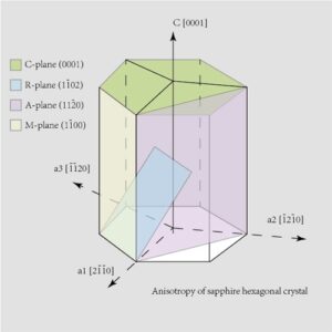
Material and Crystal Properties
Material Composition
Al₂O₃ content above 99.99% ensures outstanding purity and uniformity.
This minimizes defects and enhances the reliability of thin film growth.
Crystal Growth
Produced using the Kyropoulos method for stable lattice orientation.
Crystal structure belongs to the trigonal system with a high degree of symmetry and hardness.
Orientation Options
Standard orientation is C-plane (0001).
Optional planes such as A-plane or R-plane are available on request for optical or piezoelectric applications.
Surface Condition
Mirror-polished surface with Ra ≤ 0.3 nm on polished sides.
The surface is suitable for epitaxy, lithography, and thin-film deposition.
Performance Highlights
Thermal Management
Sapphire provides strong thermal conductivity and heat resistance.
It supports GaN and AlN epitaxial layers under high power operation.
Mechanical Strength
The wafer maintains structural stability during thermal cycles and plasma processes.
It resists cracking and deformation during device fabrication.
Optical and Electrical Performance
Sapphire is transparent from UV to IR wavelengths.
It also provides excellent electrical insulation and dielectric stability.
Chemical Resistance
The surface resists acid, alkali, and plasma corrosion.
Ideal for deposition and etching environments.
Dimensional Precision
Low TTV, bow, and warp ensure smooth wafer alignment and precise pattern transfer.
Typical Applications
- LED Production: Blue, UV, and white LED chip fabrication.
- Semiconductor Devices: GaN-on-sapphire and AlN-on-sapphire structures.
- RF Electronics: Power amplifiers, microwave, and high-frequency components.
- Optical Components: Windows, lenses, and transparent protective covers.
- Research: Material testing and wide bandgap semiconductor development.
The Advantage of Off-Axis (Vicinal) Sapphire Substrates
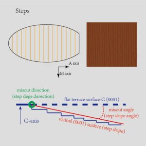
Instead of perfectly aligned crystallographic planes, off-axis (or vicinal) sapphire wafers feature a slight, intentional angular deviation during the slicing process. This creates a “terraced” micro-geometry with uniform atomic steps. For advanced materials like graphene, synthetic diamond, and MoS₂, these step edges act as crucial nucleation templates, directing crystal growth and significantly boosting the yield of large-area, single-crystal 2D layers.
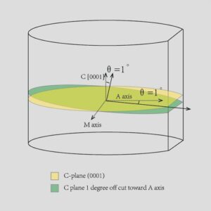
Why GaN Epitaxy Requires a C-to-M Plane Misorientation
In MOCVD production for LEDs and high-power RF components, absolutely flat substrates are counterproductive. The industry standard relies on C-plane (0001) wafers with a deliberate 0.2° to 0.3° off-cut toward the M-plane (10-10) (customizable up to 2°–3° for specialized microwave applications). This specific configuration resolves three major challenges in heteroepitaxy:
-
Optimized Step-Flow Growth: Atomic terraces provide high-energy binding sites. Instead of forming chaotic 3D islands, adatoms naturally migrate to these step edges, ensuring smooth and continuous 2D “step-flow” growth.
-
Dislocation Annihilation: To bridge the ~16% lattice mismatch between GaN and sapphire, the vicinal steps force propagating threading dislocations to bend and interact, effectively neutralizing them before they reach the active device layers.
-
Thermal Strain Management: The customized M-axis orientation helps accommodate the severe thermal stress caused by differing Coefficients of Thermal Expansion (CTE). This prevents thick epitaxial layers from cracking during the cool-down phase and ensures an epi-ready, ultra-flat surface.
Customization & Quality Assurance
- Orientation and off-cut angle customization available.
- Thickness and surface polish tailored to process needs.
- Edge bevel and chamfer according to SEMI specifications.
- 100% visual inspection and metrology verification before shipment.
- Packaging in Class 100 cleanroom environment with traceable lot control.
Advantages of Choosing This 6 Inch Sapphire Wafer
This wafer provides the balance of cost efficiency and technical performance.
It supports both pilot production and mass manufacturing.
The high purity and superior flatness improve epitaxial yield and uniformity.
It is a trusted choice for LED, optical, and high-frequency electronic systems.
Looking for larger diameters?
Check our 8 Inch Sapphire Wafers and 12 Inch Sapphire Wafers for next-gen semiconductor manufacturing.
Frequently Asked Questions (FAQ)
Q1: Why does GaN epitaxy require a specific off-axis angle (C-plane off M-plane)?
A: In mass production MOCVD processes, a perfectly flat substrate can lead to unwanted 3D island growth. Implementing a deliberate 0.2° to 0.3° off-cut toward the M-plane creates a uniform atomic terrace micro-geometry. This promotes smooth 2D step-flow growth, forces threading dislocations to bend and annihilate, and effectively manages the severe thermal stress caused by the Coefficient of Thermal Expansion (CTE) mismatch, preventing the epitaxial layers from cracking.
Q2: What are the surface polishing and cleanliness standards for these substrates?
A: We provide both Single Side Polished (SSP) and Double Side Polished (DSP) wafers. The polished surfaces undergo advanced Chemical Mechanical Polishing (CMP) to achieve a roughness of Ra ≤ 0.3 nm, strictly reaching Epi-ready standards. The final cleaning and packaging processes are completed in a Class 100 cleanroom, fully complying with the stringent environmental controls required by world-class fabrication sites.
Q3: What are the main application scenarios for this 150mm sapphire wafer?
A: Offering high optical transmission from UV to IR wavelengths, excellent resistance to acid/alkali and plasma corrosion, and superior dielectric stability, this substrate is widely utilized in blue/UV LED chip fabrication, RF microwave devices (such as power amplifiers), GaN/AlN heteroepitaxial structures, as well as high-performance optical windows and lenses.