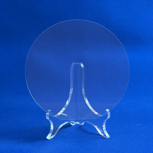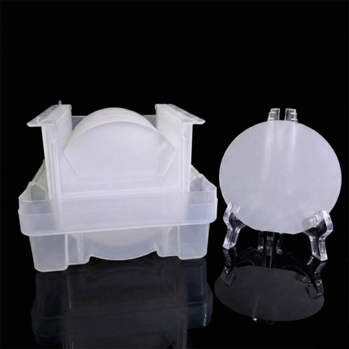
4-Inch Sapphire Double-Side Polished (DSP) Wafers
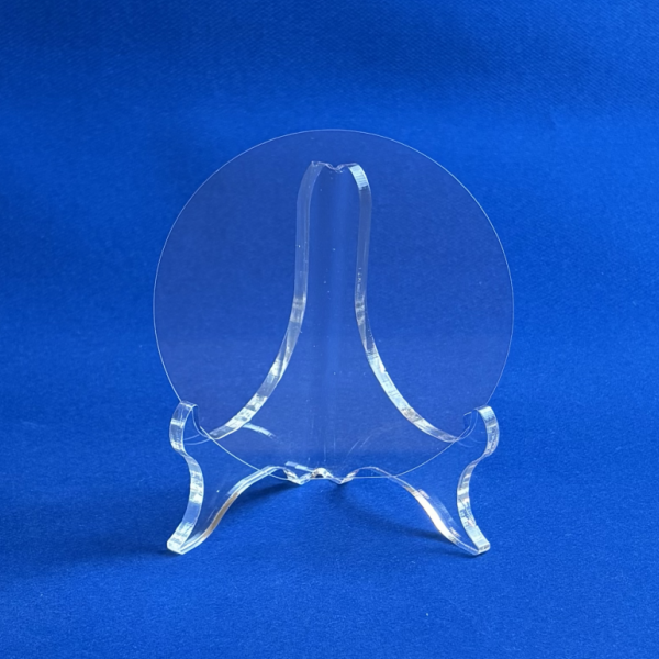
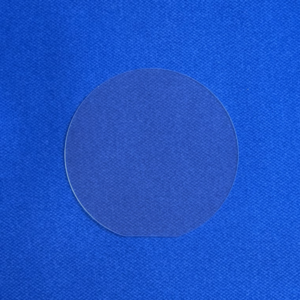
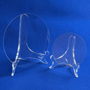
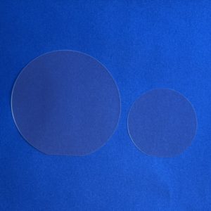
Looking for reliable, high-purity 4-inch Sapphire DSP (Double-Side Polished) Wafers for urgent research or production needs? We maintain an extensive inventory of diverse specifications available with no minimum order quantity (MOQ 1 piece). All in-stock wafers undergo rigorous cleaning and quality inspection before shipping within 1 week, ensuring your high-priority projects stay on schedule.
Why Choose Our Sapphire Wafers?
1. Superior Crystal Quality via Tungsten Thermal Field Technology
Our sapphire crystals are grown using advanced Tungsten Thermal Field (Kyropoulos / Czochralski) growth furnaces rather than traditional graphite systems:
-
Lower Impurities & Minimal Internal Stress: Substantially reduces the risk of wafer breakage during downstream processing, dicing, or micro-fabrication.
-
Exceptional Optical Clarity: Virtually free of internal micro-bubbles and cloudiness, making them ideal for applications requiring high optical transmittance.
Learn more about the advantages of Tungsten vs. Graphite Thermal Fields
2. High-Temperature Annealing (1500°C)
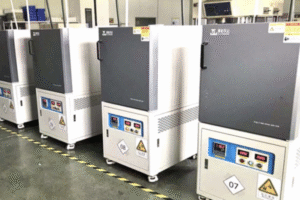
Every wafer undergoes a specialized 1500°C high-temperature annealing process, which eliminates lattice strain, stabilizes the crystal structure, and guarantees optimal performance under extreme operational conditions.
3. Advanced Chemical Mechanical Polishing (CMP)
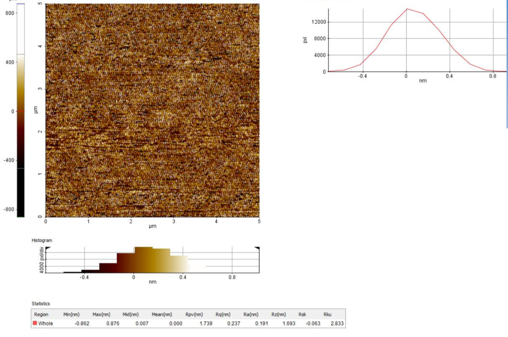
Processed with high-precision CMP equipment, our wafers achieve an atomic-level surface smoothness with a roughness of < 0.3 nm:
-
Ultra-Flat & Defect-Free Surface: Significantly lowers interface defect density, optimizing atomic layer deposition (ALD) and epitaxial film growth (e.g., GaN).
-
Enhanced Optical & Mechanical Performance: Reduces light scattering to achieve maximum optical throughput, while improving surface bond strength for wafer bonding applications.
Typical Application Cases & Success Stories
1. Optical Applications (e.g., Optical Windows, Laser Covers, & IR Sensors)
-
Specific Use Cases: High-power laser protection windows, optical viewports, infrared (IR) sensor substrates, and precision optical lenses operating in harsh environments.
-
Why Our Wafers Fit: Grown via advanced tungsten thermal fields, our sapphire crystals offer exceptionally high optical transmission (from UV to mid-IR) and superior thermal stability.
-
Case in Point: A photonics R&D team recently utilized our in-stock 4-inch DSP sapphire wafers to rapidly secure 5 test pieces. They completed preliminary optical transmission feasibility validations within days instead of waiting 4 to 6 weeks for standard custom production, drastically cutting down their project timeline and opportunity costs.
2. Epitaxial & Carrier/Tray Applications (e.g., GaN Growth & Wafer Carriers)
-
Specific Use Cases: Substrates for GaN-based LED and micro-LED epitaxy, RF integrated circuit substrates (SOS – Silicon-on-Sapphire), and high-temperature semiconductor wafer carrier trays/boats.
-
Why Our Wafers Fit: Low internal stress significantly minimizes bowing, warping, and the risk of thermal shock cracking during high-temperature epitaxial growth.
-
Case in Point: An advanced semiconductor lab required pristine substrates for thin-film and 2D material growth. Thanks to our rigorous Class 100 cleanroom processing, high-precision CMP (Ra< 0.3 nm), and advanced cleaning protocols (such as CRC100 level), our wafers arrived with virtually zero surface particles or organic contamination—allowing the engineers to achieve immediate, out-of-the-box usage without preliminary cleaning friction.
3. High-Temperature Sensors & Dry Etching (e.g., Hotplate Sensors)
-
Specific Use Cases: Hotplate sensors operating up to 1000°C, and substrates designed to withstand harsh fluorine-based dry plasma etching environments.
-
Why Our Wafers Fit: With a melting point of 2040°C and 1500°C high-temperature annealing, our wafers offer extraordinary structural integrity, chemical durability, and high-temperature dimensional stability.
-
Case in Point: A university research group developing high-temperature micro-sensors needed stable 100mm substrates with mirror-smooth CMP finishes for fine-line photolithography. By pulling directly from our stock with no MOQ constraints, they accelerated their prototyping phase immediately.
Basic Material Properties of Sapphire (Al2O3)
| Property | Value |
| Chemical Formula | Single Crystal Al2O3 (99.99% purity) |
| Crystal Structure | Hexagonal / Rhombohedral |
| Density | 3.98 g/cm^3 |
| Mohs Hardness | 9 (Scratch-resistant, second only to diamond) |
| Melting Point | 2040°C |
| Thermal Conductivity | ~40 W/(m·K) @ 25°C |
| Transmission Range | ~0.17 to 5.5 µm (UV to Mid-IR) |
| Dielectric Constant | 9.3 – 11.5 |
Typical Specifications (4-Inch Sapphire DSP Wafer)
-
Diameter: 100.0 mm
-
Orientation: C-plane (0001) off-axis or A-plane, R-plane, M-plane available
-
Thickness: 430 um, 500 um, 650 um or customized
-
Surface Finish: Double-Side Polished (DSP), Ra < 0.3 nm
-
TTV / Bow / Warp: < 10 um
-
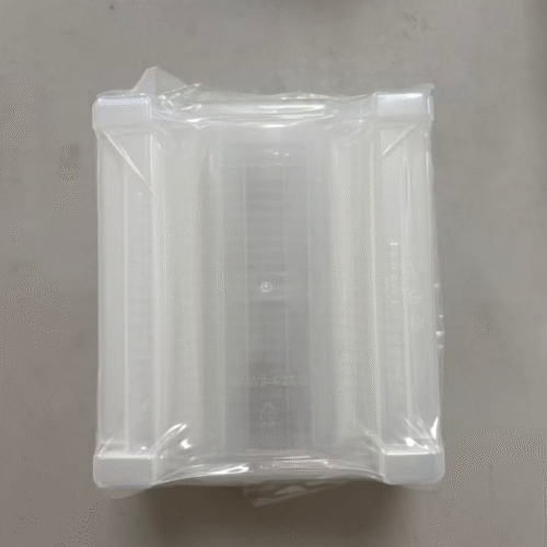
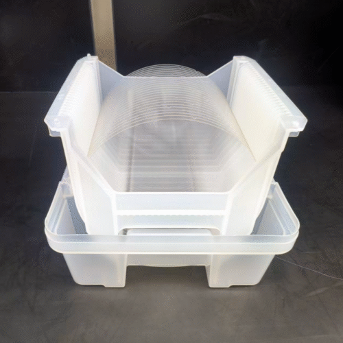
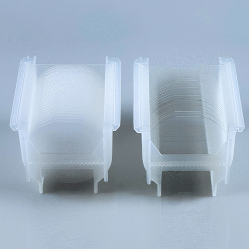
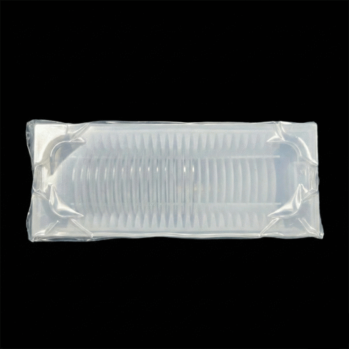
Cleanliness: Class 100 cleanroom vacuum sealed packaging (Single wafer boxes or cassette jars)
Explore Other Sapphire Wafer Sizes
Looking for a different dimension? Check out our complete range of high-precision sapphire substrates: