The Evolution of Synthetic Sapphire and the KY Method
Synthetic sapphire—often referred to as industrial sapphire or single crystal alumina—is a foundational material driving innovation in modern high-tech industries. Prized for its extreme hardness, thermal stability, and exceptional purity, it has become indispensable in advanced optics and microelectronics. However, not all synthetic sapphire is created equal; the material’s performance relies heavily on how it is grown.
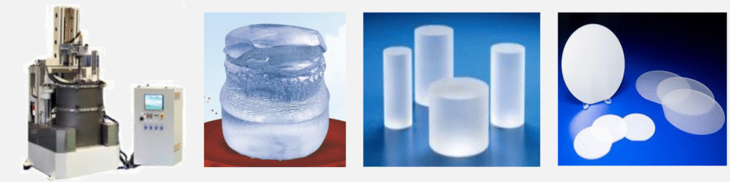
For the most critical semiconductor and electro-optical applications, the Kyropoulos (KY) method is globally recognized as the gold standard for producing large-diameter, flawless single crystals. Unlike traditional techniques that pull the crystal out of a crucible, the KY method precisely controls a thermal gradient, allowing the sapphire to grow downwards into the molten alumina. This highly controlled, slow-growth environment minimizes thermal stress, resulting in a crystal with exceptionally low dislocation density, zero porosity, and superior structural integrity.
Key Performance Parameters of KY Synthetic Sapphire
For engineers and researchers evaluating substrate materials, the data speaks for itself. The KY method produces sapphire with the following rigorous physical, thermal, and chemical properties:
| Property | Value | Unit | Significance in Manufacturing |
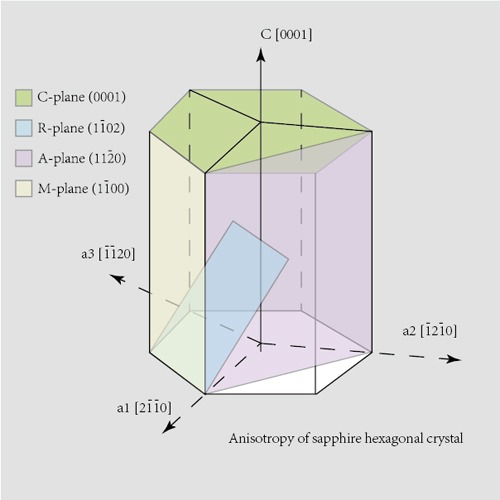
| Crystal Structure | Hexagonal (Rhombohedral) | – | Defines epitaxial growth orientation (e.g., C-plane, A-plane). |
| Density | 3.98 | g/cm³ | Ensures robust structural stability during rapid rotation in epitaxy. |
| Hardness | 9.0 (Mohs) / 22.5 GPa | Mohs / GPa | Extreme scratch resistance; requires specialized diamond tooling. |
| Melting Point | 2040 | °C | Thrives in ultra-high temperature CVD and MOCVD processes. |
| Thermal Conductivity | 42 | W/(m·K) (at 20°C) | Efficient heat dissipation for high-power electronic devices. |
| Dielectric Constant | 9.3 to 11.5 | @ 1 MHz | Excellent electrical insulation, critical for RF and microwave ICs. |
| Chemical Resistance | Inert to acids/alkalis | – | Withstands aggressive plasma and wet etching without degrading. |
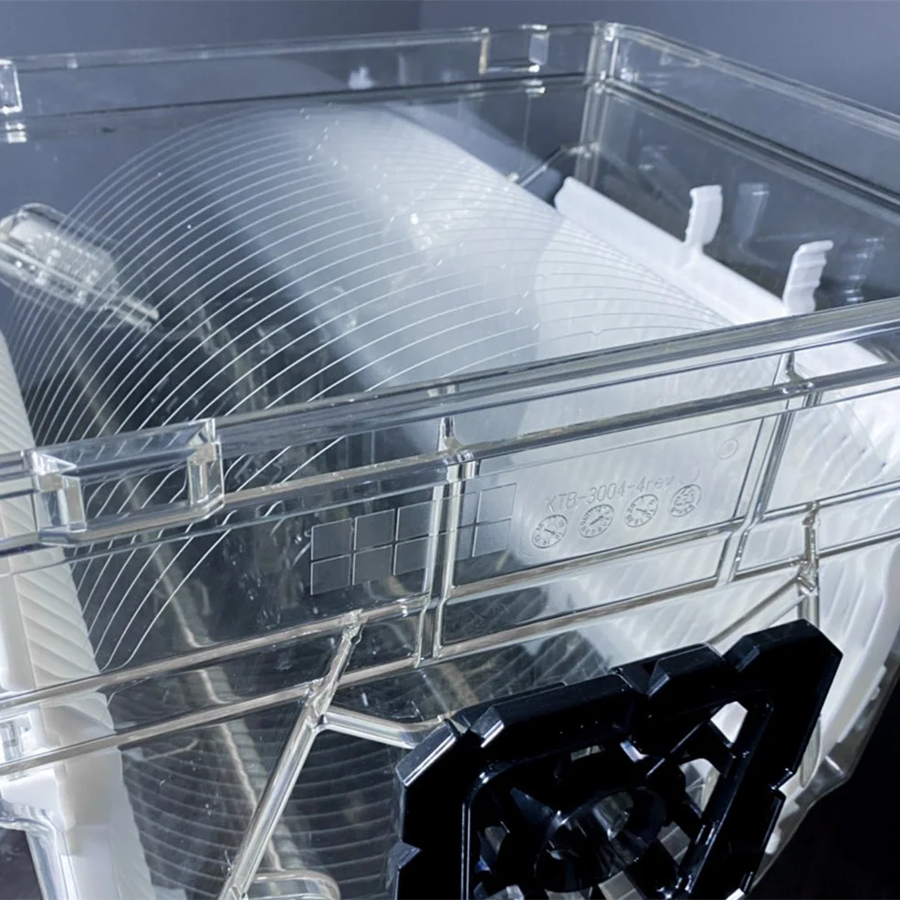
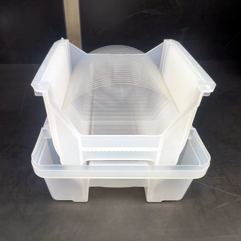
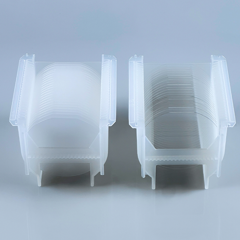
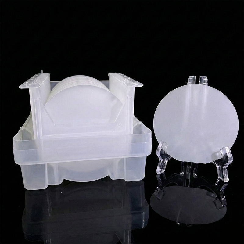
The Critical Role of Sapphire Wafers in Semiconductors
Once industrial sapphire boules are cored, sliced, and polished into wafers, they become foundational components in modern microelectronics and photonics. Their primary applications include:
Epitaxial Substrates for GaN (Gallium Nitride): Sapphire is the most widely used substrate for growing GaN-based devices. Its stable lattice structure and thermal properties make it indispensable for manufacturing high-brightness Blue/White LEDs, Micro-LED displays, and next-generation laser diodes.
Silicon-on-Sapphire (SOS) for RF Integrated Circuits: Because sapphire is a perfect electrical insulator, depositing a thin layer of silicon on a sapphire wafer (SOS technology) virtually eliminates parasitic capacitance. This results in ultra-fast, radiation-hardened microchips that are essential for 5G/6G telecommunications, aerospace, and advanced microwave systems.
High-Performance Carrier Wafers: In advanced semiconductor packaging (like Wafer-Level Packaging) and substrate thinning processes, sapphire is utilized as a carrier wafer. Its rigidity prevents the warping of ultra-thin silicon wafers, while its high optical transmission allows for easy laser de-bonding.
Advanced Applications: Off-Cut (Miscut) Sapphire Substrates & Epitaxial Growth Control
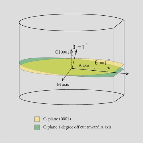
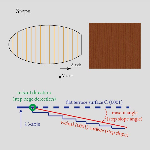
An off-cut (or miscut) sapphire substrate refers to a specialized wafer that has been intentionally sliced at a slight angle deviating from a specific crystallographic orientation (such as the C-axis, R-axis, or A-axis). This precise cutting process creates a highly regular, step-like surface structure, often referred to as atomic terraces.
These atomic-level steps enable precise directional control for subsequent epitaxial growth and surface treatments. For instance, during the single-crystal growth of 2D materials like molybdenum disulfide (MoS₂), the atomic arrangement at the step edges breaks energy degeneracy, thereby facilitating high-yield, unidirectional domain growth. Thanks to this unique microstructural advantage, miscut sapphire substrates are now widely utilized in the advanced research and manufacturing of 2D materials, high-quality diamond, graphene, and other next-generation semiconductors.
Case Study: Why is a Miscut Angle Essential for GaN Epitaxy?
In the MOCVD epitaxial growth of Gallium Nitride (GaN) for LEDs, RF microwave devices, and High Electron Mobility Transistors (HEMTs), perfectly flat sapphire substrates are rarely used. Instead, the industry standard relies on C-plane (0001) substrates miscut toward the M-plane (10-10) by approximately 0.2° to 0.3° (with off-cut angles reaching 2° to 3° for specific microwave devices or specialized high-angle processes).
This targeted miscut design addresses three critical technical challenges in semiconductor manufacturing:
Enabling Step-Flow Growth Mode: On a perfectly flat surface, epitaxial atoms nucleate randomly, leading to 3D island growth and generating numerous grain boundary defects upon coalescence. The “atomic steps” created by the misorientation provide high-surface-energy binding sites for GaN adatoms. These atoms preferentially attach to the step edges and smoothly advance along the terraces, achieving high-quality, low-defect 2D “step-flow” growth.
Reducing Threading Dislocation Density (TDD): There is an approximate 16% lattice mismatch between sapphire and GaN. The stepped structure of the miscut surface induces the dislocations in the initial nucleation layer to bend and annihilate at the steps. This effectively prevents threading dislocations from propagating upward into the active region, significantly enhancing the epitaxial wafer’s optical and electrical performance.
Thermal Stress Relief & Morphology Control: During the cooling phase following high-temperature growth, an appropriate off-cut angle (particularly toward the M-plane) helps release the immense thermal stress caused by the difference in Coefficients of Thermal Expansion (CTE), preventing the epitaxial film from cracking. Furthermore, it effectively suppresses the excessive bundling of macro-steps, ensuring a mirror-flat, production-ready surface.
About MinnOptics: Leading the Future of Large-Diameter Substrates
At MinnOptics, our value proposition is built entirely on scientific rigor, strict metrology, and direct factory manufacturing excellence. We reject empty marketing terminology in favor of verifiable data and uncompromised quality control.
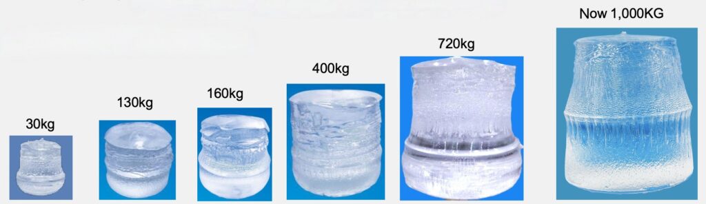
As the demands of the semiconductor industry scale, so do our capabilities. Through continuous technical innovation and facility expansion, MinnOptics is currently the only factory in the world mass-producing 12-inch sapphire wafers. By offering true factory-direct sourcing for these massive, high-purity substrates, we empower global semiconductor firms to achieve unprecedented economies of scale, maximize their epitaxial yields, and drive the future of advanced microelectronics.
Explore our sapphire substrates