We use cookies to enhance your browsing experience, serve personalized ads or content, and analyze our traffic. By clicking "Accept All", you consent to our use of cookies.
In the highly demanding fields of optoelectronics, high-power lasers, and advanced microelectronics, sapphire crystal quality is non-negotiable. Whether used as a substrate for GaN epitaxy or as a durable optical window, even a microscopic flaw can lead to catastrophic failure in downstream manufacturing.
To help engineers and procurement managers navigate these challenges, we have compiled this comprehensive guide to sapphire wafer defects. This guide is rooted in collaboratively developed semiconductor materials standards. While initially codified as a national standard, these precise defect classifications reflect a universal industry consensus, making it a highly authoritative reference for sapphire applications globally.
Quick Reference: Ingot vs. Processing Defects
Category
Origin
Can it be fixed?
Typical Examples
Ingot Defects
Formed inside the furnace during high-temp crystal growth.
❌ No (Permanent internal lattice damage)
Bubbles, Stress, Cracking, Devitrification
Processing Defects
Introduced during downstream mechanical/chemical machining.
⚠️ Sometimes (Through further polishing)
Scratches, Pits, Orange Peel, Haze
Deep Dive into Crystal Perfection: Want to understand how we measure the ultimate structural integrity of an ingot? Read our hardcore technical breakdown: [Understanding Etch Pit Density (EPD) in Sapphire: A Deep Dive into Dislocations]
Part 1: Ingot Defects (Internal and Structural Flaws)
Ingot defects (or boule defects) are born in the furnace. Because these defects are deeply embedded within the crystal lattice, they are fundamentally impossible to fix once the boule has cooled.
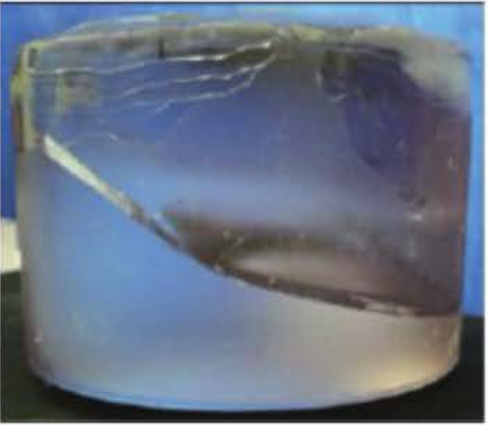
1. Cracking (Thermal Stress Failures)
What it looks like: Complete external shape, but visible fractures within the crystal interior or along the side walls.
Root Cause: Poor thermal field configuration, rapid temperature fluctuations causing massive internal thermal stress, or the crystal adhering to the crucible.
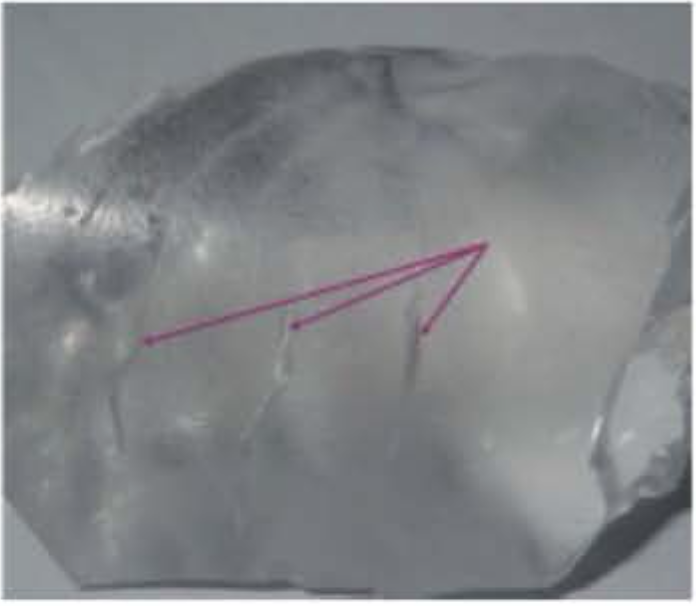
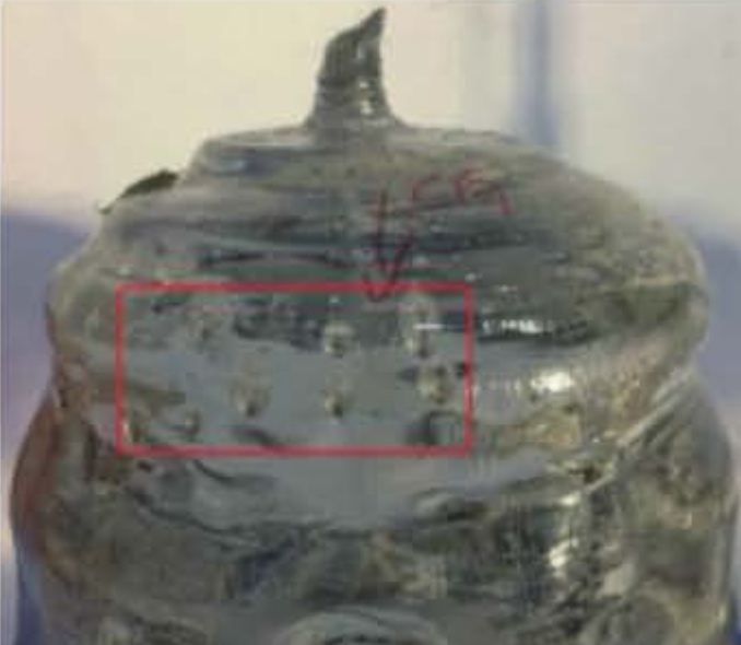
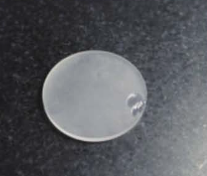
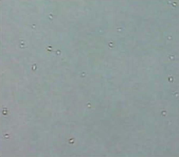
2. Bubbles and Hollows
What it looks like: Individual spherical pockets, misty cloud-like clusters, or large vacuum cavities inside the crystal.
Root Cause: Unstable melt convection failing to sweep gases away from the solid-liquid interface. A too-fast crystallization rate traps these gases permanently.
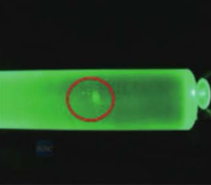
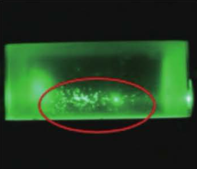
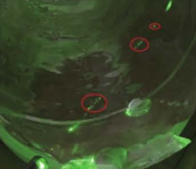
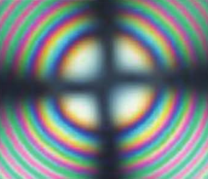
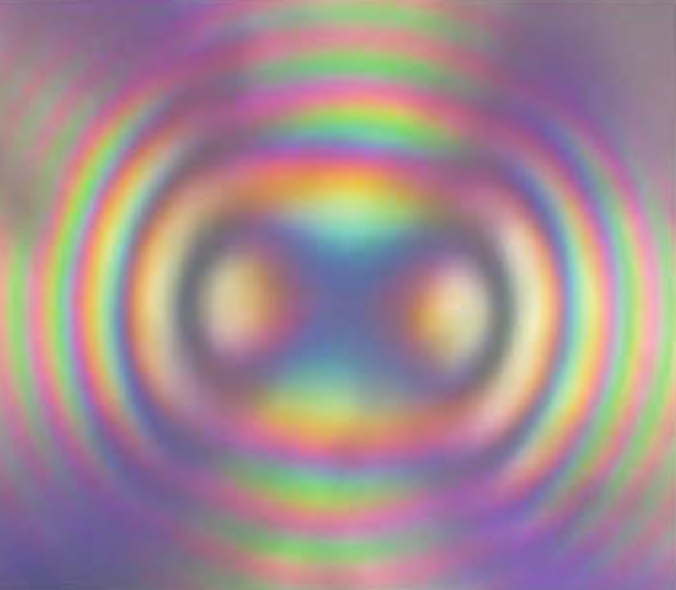
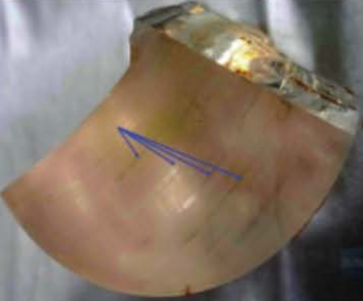
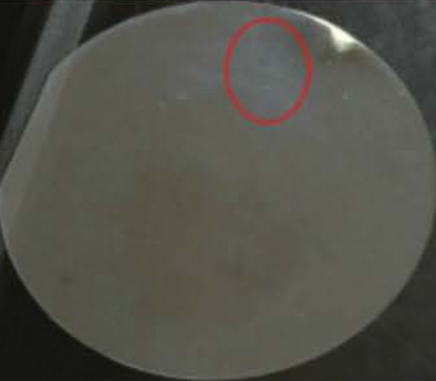
3. Internal Stress & Scattering Particles
What it looks like: Distorted optical axis figures under a stress viewer, or bright specular flares appearing along a laser path (Tyndall effect).
Root Cause: Uneven thermal strain during growth, or external mechanical vibrations embedding trace impurities into the lattice. High stress drastically lowers the Laser Induced Damage Threshold (LIDT).
Optical Engineers: Are you sourcing windows for high-power lasers? See how we eliminate these specific issues in our guide: [Optical Sapphire Quality: Managing Bubbles, Scattering, and Internal Stress]
Part 2: Processing Defects (Mechanical and Surface Flaws)
Slicing the incredibly hard (Mohs 9) yet brittle sapphire into wafers, followed by lapping and Chemical Mechanical Polishing (CMP), is a violent process. If not strictly controlled, it leaves critical surface flaws.
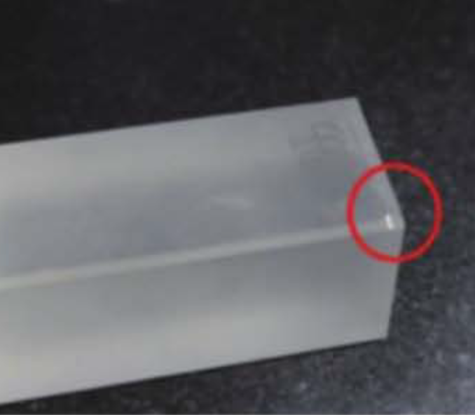
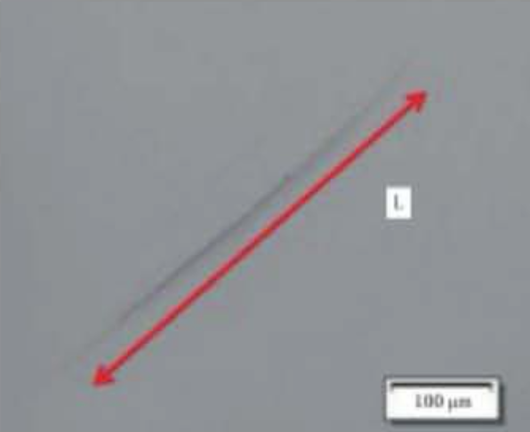
1. Cutting Marks and Chipping
What it looks like: Alternating concave/convex grooves on the surface, or localized breakage along the wafer’s edge.
Root Cause: Wobbling diamond wire saws or inconsistent cutting speeds create marks. Edge chipping occurs when internal edge stress is released during slicing or lapping.
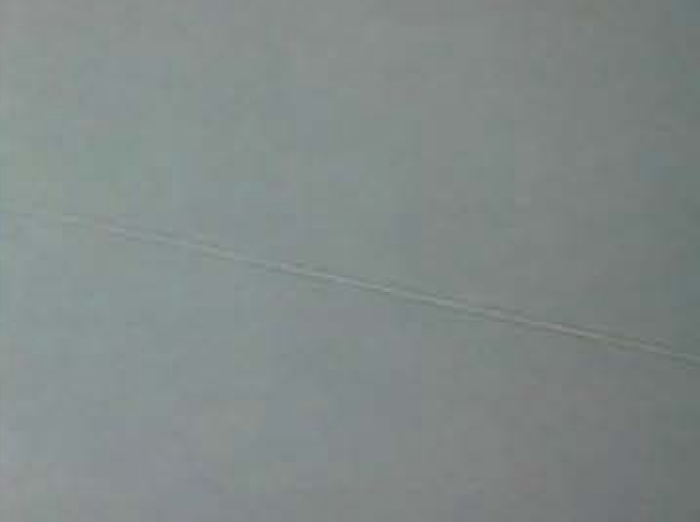
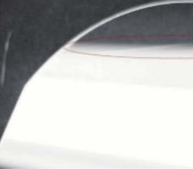
2. Pits and Scratches
What it looks like: Irregular linear grooves (scratches) or small bright pockmarks (pits/dimples) across the polished surface.
Root Cause: Oversized hard particles contaminating the lapping slurry. Pits occur when the mechanical Sub-Surface Damage (SSD) from rough grinding isn’t fully removed, and the CMP chemicals preferentially etch those micro-fractures into visible dimples.
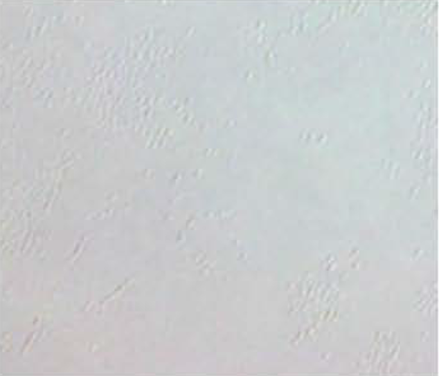
3. Waviness (Orange Peel) and Polishing Haze
What it looks like: A textured, dimpled look resembling water ripples/orange peel, or a macroscopic smoke-like cloudiness (diffuse reflection).
Root Cause: For epitaxial growth, the surface must be atomically flat. If the chemical etching action in the CMP slurry outpaces the mechanical abrasion (often due to incorrect pH levels), it destroys the surface flatness, causing haze and lattice mismatches during GaN deposition.
Why Strict Standards Matter
Mastering sapphire manufacturing requires a deep understanding of both thermodynamic growth and sub-micron mechanical processing. By relying on internationally recognized semiconductor materials standards and rigorous inspection protocols, manufacturers can eliminate these defects at the source.
Tired of hidden defects ruining your yield?
Our quality control processes strictly adhere to these universal industry standards, ensuring zero-haze, low-stress, and perfectly polished wafers.
Explore Our Defect-Free Sapphire Solutions
Whether you are growing LEDs, manufacturing RFICs, or building high-power laser optics, we have a meticulously inspected substrate for your application: