Product Overview
The 12 inch sapphire substrate from MinnOptics is a precision-engineered wafer for semiconductor and optoelectronic manufacturing.
It is produced using single crystal aluminum oxide (Al₂O₃) with purity above 99.999%.
The substrate is only available in DSP (Double Side Polished) formats.
Each wafer is manufactured with strict control of orientation, thickness, and flatness to meet advanced device process needs.
12 Inch Sapphire Wafer Specification
| Parameters | Specifications |
| Material | High Purity Single Crystal Al2O3 |
| Crystal Growth Method | Kyropoulos (KY) Method |
| Orientation | C-plane (0001) (Off-axis available) |
| Diameter | 300.0 ± 0.2 mm |
| Thickness | 500 – 1500 um ± 25 um (Customizable) |
| Notch Orientation | A-plane |
| TTV | ≤ 10 um |
| Bow | ≤ 50 um |
| Warp | ≤ 150 um |
| Surface Finish (Front) | Epi-ready, CMP Polished, Ra≤ 0.3 nm |
| Surface Finish (Back) | Epi-ready, CMP Polished, Ra≤ 0.3 nm |
| Edge Profile | SEMI Standard Bevel |
| Cleanliness | Class 100 Cleanroom Packed |
| Packaging | FOSB (Front Opening Shipping Box) |
Material Characteristics
Crystal Structure
Sapphire belongs to the trigonal system and is grown by the Kyropoulos method.
It exhibits strong mechanical and thermal properties suitable for high-precision fabrication.
Chemical Composition
Material: Al₂O₃ ≥ 99.999%.
This high purity ensures minimal impurities, low lattice defects, and stable epitaxial growth.
Orientation Options
Standard: C-plane (0001).
Surface Finish
DSP: Both sides polished to mirror quality for double-sided processing.
Understanding Why 12-Inch Sapphire Wafers are Only Available in DSP
Performance Advantages
Thermal Conductivity
Sapphire provides superior thermal transfer, reducing device heat accumulation.
This supports efficient LED and power semiconductor performance.
Mechanical Strength
High hardness (Mohs 9) and excellent scratch resistance make sapphire ideal for high-throughput processing and repeated thermal cycles.
Optical Transparency
Wide transparency from UV to IR enables use in optical sensors, lenses, and display components.
Chemical Resistance
Stable under acids, alkalis, and plasma exposure.
Suitable for deposition, etching, and high-temperature annealing.
Dimensional Stability
The wafer maintains geometry under high stress.
This supports consistent device alignment and uniform epitaxial layers.
Application Areas
- Semiconductor Substrate: GaN, AlN, and other compound semiconductor epitaxy.
- LED Manufacturing: Blue, green, and white LED production lines.
- Optical Components: Windows, lenses, and IR transmission elements.
- RF and Power Devices: GaN-on-Sapphire, RF amplifiers, and high-voltage modules.
- Research and Development: Wafer-scale optical and thermal studies.
Customization Options
MinnOptics provides flexible customization to meet process requirements:
- Thickness range from 500 µm to 1500 µm.
- Orientation adjustment (on-axis or off-axis).
- Surface treatment including CMP and ultra-flat polishing.
- Edge profile (bevel or chamfer) according to SEMI standards.
All wafers are packed in Class 100 cleanroom conditions and shipped with complete inspection reports.
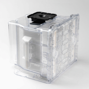
Packaging & Shipping
Unlike 2-8 inch wafers that use standard cassettes, our 12-inch (300mm) sapphire substrates are packed in professional FOSB (Front Opening Shipping Box).
- Maximum Protection: Designed to prevent contamination and vibration during transit.
- Cleanroom Ready: All wafers are packed in Class 100 cleanroom environments.
- Industry Standard: Fully compatible with automated semiconductor handling equipment.