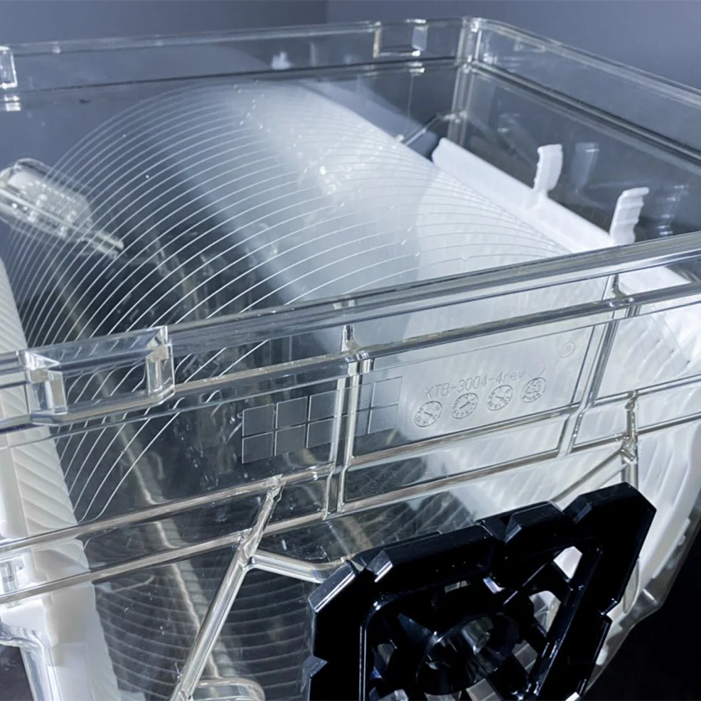
The semiconductor industry is entering an era where device geometries continue to shrink and manufacturing complexity increases. In this environment, wafer cleaning has become one of the most critical steps in ensuring yield, reliability, and long-term device performance. As the demand for higher purity and more resilient substrates rises, sapphire wafers are receiving renewed attention from engineers and manufacturers.
Growing Importance of Wafer Cleaning in Modern Fabs
Contamination has become a major obstacle in advanced semiconductor production. Even microscopic particles and thin layers of organic or metallic residue can disrupt the electrical characteristics of a device. This is especially true for feature sizes below 20 nanometers.
Cleaning now appears throughout the entire production flow. It is performed before film deposition, after etching, after ion implantation, and after CMP polishing. In many mature process lines, cleaning can represent close to one third of the total number of manufacturing steps.
As technology nodes become smaller, the number of cleaning cycles increases. Some older nodes such as 90 nanometers may require about ninety cleaning steps. Leading-edge nodes can go beyond two hundred cleaning steps in a single production route.
Two Major Categories of Cleaning Technology
Current semiconductor fabs use two primary cleaning approaches. The first category is wet cleaning. This involves chemical solutions or highly purified water. Traditional immersion baths and spray-type systems are both widely used for removing particles and chemical residues.
The second category is dry cleaning. Plasma treatments and gas-phase reactions remove organic material, particles, and oxide layers without using large quantities of liquid chemicals. This approach is becoming attractive for facilities that want to reduce wastewater generation.
Common Wet Cleaning Techniques
- Several standard wet cleaning chemistries continue to dominate semiconductor production.
- Deionized water provides particle removal and rinsing while minimizing corrosion.
- Hydrofluoric acid is widely used for removing native oxide layers such as silicon dioxide.
- The SC-1 solution made from ammonium hydroxide, hydrogen peroxide, and water removes organic contaminants and particles. Many fabs use ultrasonic or megasonic energy to improve cleaning efficiency.
- The SC-2 mixture made from hydrochloric acid, hydrogen peroxide, and water focuses on eliminating metallic contamination.
- Ozone-based cleaning methods oxidize organic residues while avoiding the creation of harmful by-products.
- Organic solvents are used when delicate surfaces cannot tolerate stronger acids or bases.
Advanced and Emerging Cleaning Technologies
Megasonic cleaning uses very high frequency acoustic energy that creates microscopic cavitation bubbles. These bubbles remove particles more gently than traditional ultrasonic cleaning and are suitable for fragile structures.
Dry plasma cleaning uses oxygen or inert gases to remove organic layers or oxide films with high precision. This avoids the need for chemical waste treatment.
High-end fabs now rely on surface analysis tools such as XPS, AFM, and SEM to evaluate cleaning quality at the nanoscale.
Cleaning Challenges Specific to Sapphire Wafers
Sapphire substrates provide excellent hardness and chemical stability. These same properties also make them more difficult to clean compared with silicon. Sapphire does not react easily with many standard cleaning chemicals. As a result, wafer manufacturers often combine acidic and alkaline solutions with ultrasonic processing to achieve the required level of surface purity.
Research involving GaN growth on sapphire also uses oxygen plasma and hydrogen plasma treatments to remove organic layers. RCA-based methods such as SC-1 and SC-2 can help eliminate metallic contaminants on sapphire surfaces.
Patented cleaning sequences for sapphire often include soaking, ultrasonic activation, precision rinsing, and spin drying. Each step is designed to maintain surface integrity while improving cleanliness.
Why High-Quality Sapphire Wafers Are Essential
- Sapphire wafers must withstand repeated cleaning cycles without surface damage. This is critical for optoelectronic, RF, LED, and other high-performance applications.
- High-purity sapphire substrates support advanced cleaning processes by maintaining surface flatness and chemical stability.
- Improved wafer quality reduces defect rates and increases the efficiency of downstream manufacturing steps.
Our Sapphire Wafer Solutions
If you require sapphire wafers engineered for superior purity, smoothness, and compatibility with modern cleaning processes, our products can support your production needs.

