Product Overview
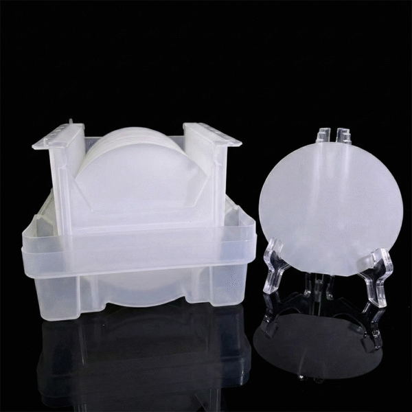
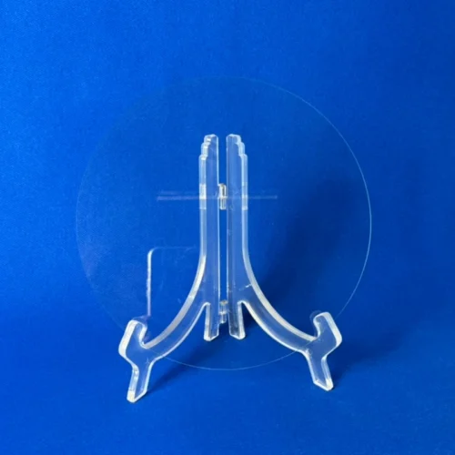
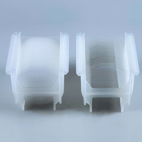
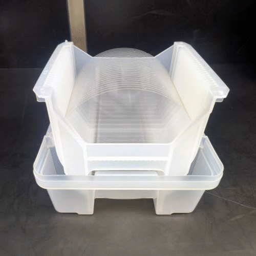
The 4 inch sapphire substrate is a reliable base material for semiconductor, LED, and optical device production.
It is produced from single crystal aluminum oxide (Al₂O₃) grown with high precision technology.
Each wafer offers excellent hardness, thermal stability, and optical clarity.
Available in SSP (single side polished) and DSP (double side polished) forms, this substrate is widely used in both R&D and mass production lines.
Material Properties
Crystal Composition
High purity Al₂O₃ (≥ 99.999%) with low impurity content.
Stable crystalline structure ensures consistent lattice alignment for epitaxial layers.
Growth Method
Fabricated using Kyropoulos growth techniques to maintain uniform crystal orientation and minimal defects.
Crystal Orientation
Standard: C-plane (0001).
Alternative orientations such as A-plane or R-plane available upon request.
Surface Quality
Mirror finish on polished surfaces.
Surface roughness Ra ≤ 0.3 nm ensures superior adhesion and low defect density in thin films.
Key Features
High Thermal Conductivity
Sapphire offers efficient heat transfer, which supports high-power operation and LED chip cooling.
Mechanical Strength
With high hardness (Mohs 9), sapphire resists mechanical damage during processing and device packaging.
Optical Transmission
Transparent in UV, visible, and IR ranges.
This makes it ideal for optical and photonic applications.
Chemical Stability
Inert to most acids, bases, and plasma gases.
Suitable for etching and deposition environments.
Excellent Planarity
Low TTV and controlled bow provide stable wafer flatness for precise lithography and epitaxy.
Application Fields
- LED Devices: GaN, AlN, and InGaN epitaxy for blue and UV LED chips.
- RF Electronics: High-frequency GaN amplifiers and power modules.
- Optical Components: Lenses, windows, and laser substrates.
- Semiconductors: Wide bandgap device development.
- Research and Development: Test wafers for epitaxial process study and calibration.
Customization Options
- Orientation customization (A-plane, C-plane, R-plane, or off-cut).
- Variable thickness from 350 µm to 600 µm.
- SSP, DSP, or etched surface finishes available.
- Edge profile and flat specifications per SEMI standards.
- Optional double-sided alignment marks or laser ID.
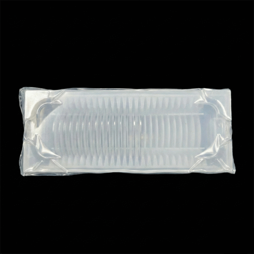
All wafers are cleaned, vacuum-packed, and delivered with full quality certification.
Advantages of 4 Inch Sapphire Wafer
The 4 inch format is ideal for laboratory research, pilot production, and specialized semiconductor applications.
It provides stable performance, easy handling, and high material reliability.
Its consistent optical and thermal properties make it a preferred substrate for GaN and LED growth.
MinnOptics ensures repeatable quality and global supply capability for sapphire wafers.
