Product Overview
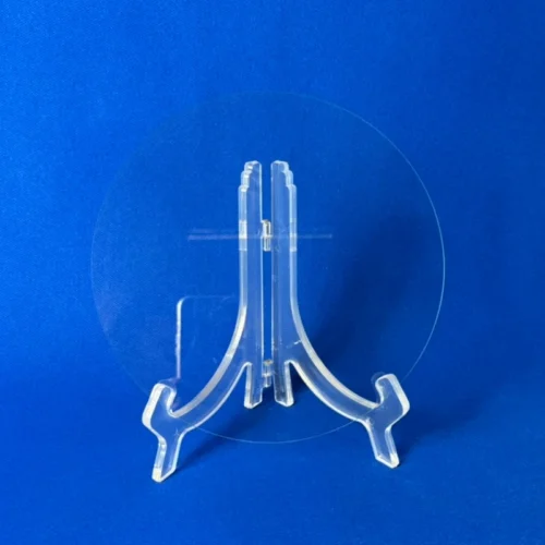
The 2 inch sapphire substrate is a precision material designed for semiconductor, LED, and optical device fabrication.
It is made from high purity single crystal aluminum oxide (Al₂O₃).
The wafer features excellent optical transmission, chemical resistance, and thermal stability.
Both SSP (single side polished) and DSP (double side polished) versions are available to match research and production needs.

Material and Crystal Properties
Material Composition
High purity Al₂O₃ with 99.999 percent purity ensures low impurity levels and minimal defects.
This purity supports high-quality epitaxial growth and long-term device stability.
Crystal Growth Method
Manufactured by Kyropoulos crystal growth techniques.
Uniform lattice structure and consistent orientation ensure stable film deposition.
Orientation Options
Standard orientation: C-plane (0001).
A-plane or R-plane options available for optical and piezoelectric applications.
Surface Quality
Mirror-polished surface with roughness Ra ≤ 0.3 nm.
Surface uniformity guarantees better thin film adhesion and low particle contamination.
Key Features
Thermal Performance
High thermal conductivity supports efficient heat dissipation during epitaxial growth.
Mechanical Durability
Strong crystal structure resists fracture and stress during process steps.
Optical Transparency
Wide transmission range from ultraviolet to infrared.
Ideal for optical sensors, laser systems, and transparent substrates.
Chemical Resistance
Stable in acid, alkali, and plasma environments.
Suitable for high-temperature etching and coating processes.
Precision Flatness
Low bow and warp enable high-resolution lithography and precise layer control.
Applications
- LED Chips: Used as base for GaN and AlN epitaxial growth.
- RF Devices: Suitable for high-frequency and power amplifier applications.
- Optical Components: Applied in windows, mirrors, and laser substrates.
- Semiconductor R&D: Used for thin-film testing and calibration.
- Sensors and MEMS: Reliable material for precision sensing and micro devices.
Customization Options
- SSP or DSP surface finish available.
- Orientation customization including A-plane and R-plane.
- Thickness range between 300 µm and 500 µm.
- Edge shaping per SEMI standard requirements.
- Optional alignment marks or laser-engraved IDs for process traceability.
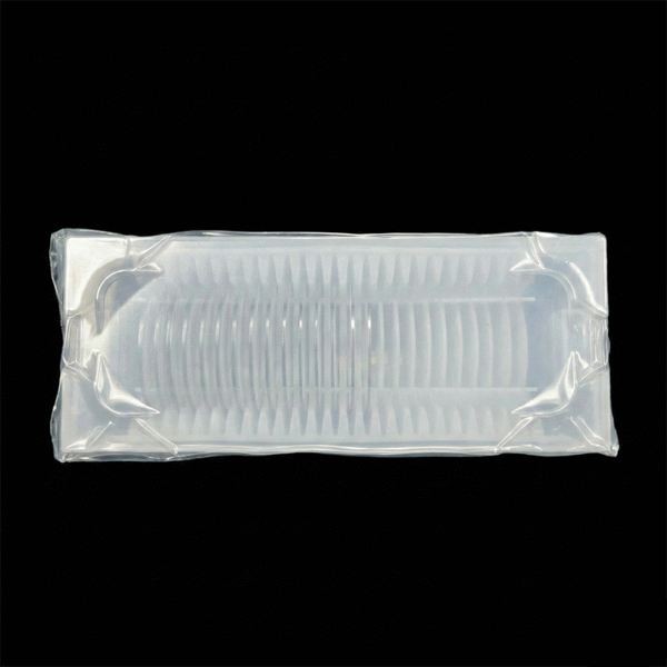
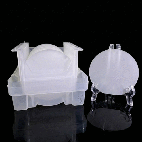
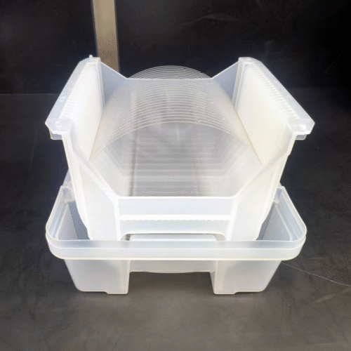
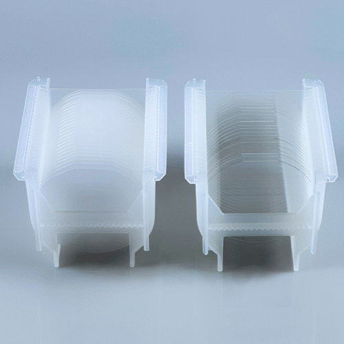
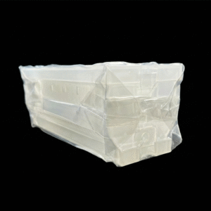
All wafers are packaged in anti-static containers and vacuum-sealed for protection.
Advantages of 2 Inch Sapphire Wafer
The 2 inch sapphire wafer is widely used for material research and prototype development.
It provides a cost-effective solution with high mechanical strength and optical clarity.
The small diameter allows easy handling in laboratory environments.
Its superior stability and flatness make it ideal for GaN-based and optical device fabrication.
