Overview
Engineered specifically for the demanding requirements of Micro LED manufacturing and advanced semiconductor packaging, our 6-inch Double Side Polished (DSP) sapphire wafer carriers deliver unparalleled mechanical stability and surface flatness.
Currently widely adopted by leading semiconductor fabs and optoelectronics production lines across South Korea and Vietnam, these high-purity sapphire carriers are the critical substrate for ensuring ultimate precision during wafer bonding, back-grinding (thinning), and mass transfer operations.
Technical Specifications
To meet the rigorous tolerance thresholds of next-generation Micro LED processes, our 6-inch sapphire carriers undergo strict quality control to guarantee exceptional Total Thickness Variation (TTV) and surface roughness.
| Parameter | Technical Specification |
| Material | High Purity Sapphire (Al₂O₃) |
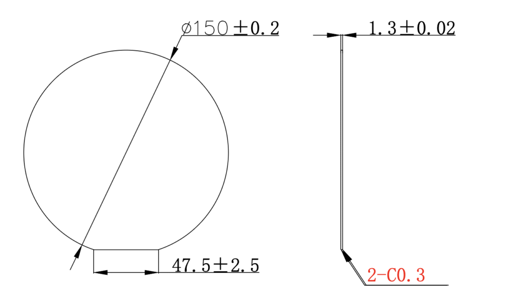
| Diameter | 150 ± 0.2 mm |
| Standard Thickness | 1300 ± 20 µm |
| Crystal Orientation | C Plane ± 0.3° |
| Primary Flat | 47.5 ± 2.5 mm |
| Surface Finish | Double Side Polished (DSP) |
| Surface Roughness (Ra) | < 0.3 nm |
| TTV (Total Thickness Variation) | < 15 µm |
| BOW | < 15 µm |
| Warp | < 25 µm |
Inventory Status and Advanced Cleaning Options
Contamination control is critical in carrier wafer applications. We provide flexible processing and fast shipping to keep your production line moving.
- In-Stock Availability: The standard 1300µm specification is currently fully stocked for immediate deployment to global manufacturing hubs.
- Ultrasonic Cleaning: Standard industrial-grade ultrasonic cleaning for general processing environments.
- CRC-100 Cleaning: Advanced CRC-100 semiconductor-grade cleaning available upon request, highly recommended for direct bonding applications to ensure a particle-free surface.
Engineering Insight: Why 1300µm is the Industry Standard for Micro LED Carriers
As the Micro LED industry scales up, the traditional 650µm or 1000µm carrier thicknesses are rapidly being replaced by the 1300µm specification. Our 1300µm DSP sapphire wafers provide four distinct manufacturing advantages:
1. Superior Mechanical Rigidity for Bow/Warp Control
Acting as the backbone during heterogeneous integration, the carrier wafer must support ultra-thin device layers across a wide 150mm span. The 1300µm thickness provides exceptional resistance to mechanical deformation, strictly keeping BOW under 15µm and Warp under 25µm under high bonding pressure. This prevents device layer cracking and alignment shifts.
2. Enhanced Thermal Stability During Bonding
Micro LED fabrication involves multiple thermal cycles. Because sapphire’s Coefficient of Thermal Expansion (CTE) differs from silicon or specific epitaxial materials, bonding often induces stress. The 1300µm thickness increases the thermal mass and structural integrity of the carrier, effectively suppressing thermal-induced warpage during high-temperature heterogeneous bonding.
3. Optimized Optical Path for Laser Lift-Off (LLO)
In GaN-based Micro LED processes, excimer lasers are utilized to penetrate the sapphire substrate and separate the device layer. The 1300µm dimension acts as an optimal optical transmission window for the focal lengths of mainstream LLO equipment. It ensures maximum UV energy transmittance while preventing localized thermal breakdown associated with thinner substrates.
4. High Reusability for Lower Total Cost of Ownership (TCO)
Sapphire carrier wafers are consumable assets that undergo repeated Chemical Mechanical Polishing (CMP) and cleaning cycles. A 1300µm substrate offers a substantial “thickness margin.” Compared to 1000µm carriers, it can endure significantly more recycling and repolishing loops before falling out of spec, drastically lowering the long-term consumable costs for your fab.
Custom Sapphire Wafer Solutions
While 1300µm is a typical thickness for 6-inch Micro LED carriers, we understand that proprietary R&D processes may require unique dimensions. We offer comprehensive custom machining, slicing, and polishing services.
Contact our engineering team today to inquire about other thicknesses, custom tolerances, or specific SEMI-standard edge profiles tailored to your semiconductor equipment.
Looking for larger diameters?
Check our 8 Inch Sapphire Wafers and 12 Inch Sapphire Wafers for next-gen semiconductor manufacturing.