Overview
The 8 inch sapphire substrate is a precision-engineered wafer designed for semiconductor and optoelectronic manufacturing.
It is made from single crystal aluminum oxide (Al₂O₃) with electronic-grade purity above 99.999%.
This wafer provides excellent flatness, high thermal conductivity, and superior mechanical strength.
Both SSP (single side polished) and DSP (double side polished) types are available to fit diverse process needs.
8 Inch Sapphire Wafer Specification
| Parameters | Specifications |
| Material | High Purity Single Crystal Al2O3 |
| Crystal Growth Method | Kyropoulos (KY) Method |
| Orientation | C-plane (0001) (Off-axis available) |
| Diameter | 200.0 ± 0.2 mm |
| Thickness | 500 – 1500 um ± 25 um (Customizable) |
| Notch Orientation | A-plane |
| TTV | ≤ 5 um |
| Bow | ≤ 25 um |
| Warp | ≤ 80 um |
| Surface Finish (Front) | Epi-ready, CMP Polished, Ra≤ 0.3 nm |
| Surface Finish (Back) | Epi-ready, CMP Polished, Ra≤ 0.3 nm |
| Edge Profile | SEMI Standard Bevel |
| Cleanliness | Class 100 Cleanroom Packed |
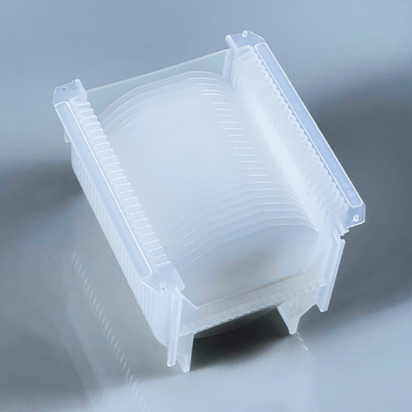
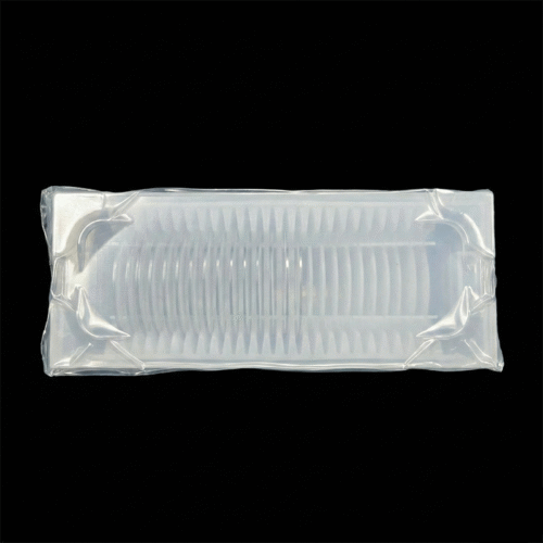
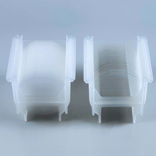
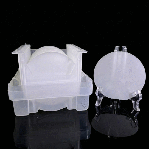
| Packaging | 8 inch Cassette (≤25 pcs) |
Material and Crystal Quality
Crystal Type
Grown by Kyropoulos methods to ensure high crystalline uniformity.
No bubbles, inclusions, or grain boundaries.
Chemical Composition
High purity Al₂O₃ with low trace metallic contamination.
This supports high-yield epitaxial growth and stable optical transmission.
Orientation Options
Standard: C-plane (0001).
Optional: A-plane, R-plane, or M-plane available for specific deposition or optical alignment.
Surface Quality
Polished using advanced CMP technology.
Surface roughness (Ra) ≤ 0.3 nm on DSP polished sides.
Excellent parallelism and thickness uniformity for thin-film growth.
Performance Advantages
High Thermal Conductivity
Sapphire efficiently transfers heat, reducing thermal stress in GaN or AlN devices.
Strong Mechanical Properties
With high hardness and fracture strength, it maintains structural integrity through thermal cycling and CMP.
Optical and Electrical Stability
Transparent from ultraviolet to infrared.
Chemically inert and electrically insulating, making it ideal for optoelectronic devices.
Dimensional Precision
Low TTV and bow improve wafer planarity, supporting accurate lithography and epitaxy.
Consistent Quality
Each wafer undergoes automatic metrology inspection and defect mapping.
Uniform results ensure repeatable performance across batches.
Applications
- Semiconductors: GaN-on-sapphire, SiC-on-sapphire, and compound semiconductor epitaxy.
- LED Production: Blue, UV, and high-brightness LED chips.
- RF Components: GaN RF amplifiers and power modules.
- Optical Systems: Windows, laser substrates, optical coatings.
- Sensor Devices: Infrared detectors, MEMS components, and piezoelectric transducers.
- Research: Wafer-scale materials testing and wide bandgap development.
Customization and Services
- Thickness available from 500 µm to 1200 µm.
- Orientation angle tolerance ≤ 0.5°.
- Bevel, edge rounding, or chamfer per SEMI standards.
- SSP, DSP, or etched surface finish available.
- Full inspection reports and traceable batch control.
Packaging is compliant with semiconductor-grade handling standards to prevent contamination and mechanical damage.
Why Choose This 8 Inch Sapphire Wafer
The 8 inch format provides an ideal balance between production efficiency and process flexibility.
It offers excellent thermal management and optical transparency.
The combination of crystal quality and precision polishing supports reliable epitaxial growth.
It is the preferred substrate for next-generation LED, RF, and high-power devices.
Looking for larger diameters?
Check our 12 Inch Sapphire Wafers for next-gen semiconductor manufacturing.
