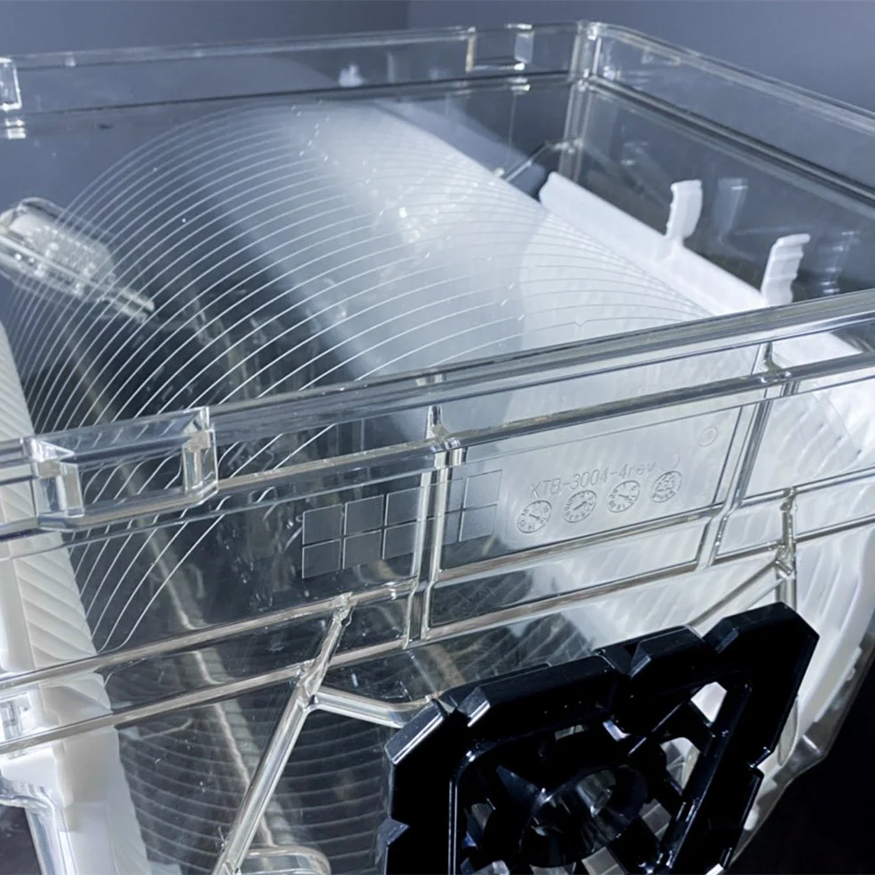
In high-performance semiconductor and optoelectronic manufacturing, sapphire wafers are widely used for LEDs, RF devices, sensors, and other advanced components. While single-side polished (SSP) wafers are common, double-side polished (DSP) sapphire wafers offer clear advantages in terms of flatness, thickness uniformity, and mechanical stability, especially for larger diameters such as 12 inches.
This article explains why DSP sapphire wafers outperform SSP wafers in key parameters including TTV, bow, warp, and TIR, and why these differences are important for high-quality wafer processing.
DSP vs SSP: The Main Difference
SSP (Single-Side Polished Sapphire Wafers): Only one surface is polished to optical quality. The backside remains lapped or roughly polished.
DSP (Double-Side Polished Sapphire Wafers): Both surfaces undergo precision polishing, resulting in mirror-like finishes on the front and back sides.
This difference may seem simple, but it significantly affects wafer geometry and mechanical properties.
Why DSP Sapphire Wafers Have Better TTV, Bow, Warp and TIR
1. Balanced Stress and Improved Bow
SSP wafers have asymmetric mechanical stress because only one side is polished. This imbalance can lead to:
Increased bow
Higher warp
Uneven thickness near the edges
DSP wafers achieve symmetrical stress distribution across the wafer by polishing both sides. This minimizes bow and improves flatness, making DSP wafers inherently more stable during handling and processing.
2. Reduced Thickness Variation (TTV)
TTV, or Total Thickness Variation, measures the difference between the thickest and thinnest points of a wafer.
In SSP wafers, the rough backside and one-sided material removal can result in larger TTV.
DSP wafers are polished on both sides, removing residual roughness and creating more uniform thickness across the entire wafer.
This is especially important for 12-inch sapphire wafers, where even small thickness variations can affect processing consistency.
3. Enhanced Warp Control
Warp measures the maximum vertical deviation across a free wafer. Large-diameter wafers are particularly susceptible to warping due to their size and internal stresses.
SSP wafers are prone to warping because of backside roughness and uneven stress distribution.
DSP wafers, with both sides polished, have reduced warp, offering more predictable mechanical performance.
Lower warp improves handling safety and reduces breakage risk.
4. Improved TIR (Total Indicated Reading)
TIR represents the maximum deviation of a wafer surface under clamping conditions.
SSP wafers with rough back surfaces may not sit evenly in vacuum chucks, leading to inaccurate TIR and potential tilt.
DSP wafers have smooth, parallel surfaces on both sides, ensuring better chuck stability, accurate metrology, and reliable processing.
This is particularly critical for automated handling and precision equipment.
5. Advantages for Large-Diameter Wafers
For 12-inch sapphire wafers, the benefits of DSP are amplified:
Large wafers are more prone to mechanical deformation.
Backside roughness in SSP wafers increases risk of breakage and uneven stress.
DSP wafers provide better flatness, lower bow and warp, and consistent TTV, which simplifies handling and improves overall yield.
In practice, DSP sapphire wafers combine mechanical stability and geometric precision, making them the preferred choice for high-performance applications.
Conclusion
Even when only one surface of a sapphire wafer is actively used, DSP sapphire wafers provide clear advantages over SSP wafers in:
TTV (Total Thickness Variation)
Bow
Warp
TIR (Total Indicated Reading)
These improvements lead to better handling, reduced breakage risk, and more consistent wafer performance, especially for 12-inch sapphire substrates.
For high-quality DSP sapphire wafers designed to meet strict flatness and mechanical specifications, visit the link below:

