Overview
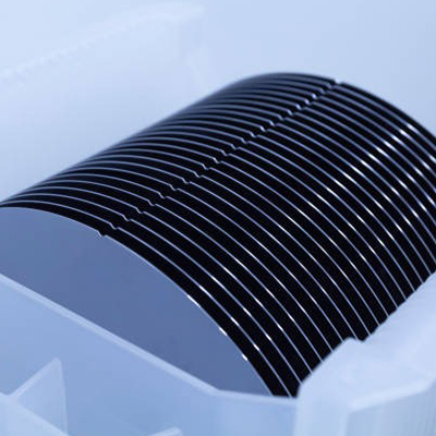
The 12 inch (300 mm) silicon carbide substrate from MinnOptics is a large size, high purity 4H-N type wafer.
It is designed for power devices, RF systems, and heat dissipation applications that require top performance under high stress.
This substrate offers excellent thermal stability and mechanical strength for advanced semiconductor manufacturing.
Main Advantages
1. Superior Heat Transfer
Silicon carbide has more than three times the thermal conductivity of silicon.
This ensures better heat management and longer device lifetime.
2. High Electric Field Strength
The breakdown field strength of 4H-SiC supports high voltage and high power operation.
It allows compact and efficient power systems.
3. Wide Bandgap Performance
With a 3.26 eV bandgap, the substrate supports high frequency and high temperature electronics.
Devices made on this substrate maintain stable performance in extreme conditions.
4. Mechanical and Chemical Stability
SiC is extremely hard and resistant to chemical corrosion.
This ensures durability and minimal wafer damage during processing.
5. Large Diameter Efficiency
The 12 inch (300 mm) size improves production yield and reduces cost per device.
It enables higher throughput for large-scale manufacturing.
6. Low Defect Density
Advanced crystal growth ensures a smooth surface and uniform structure.
This minimizes defects in epitaxial growth and device fabrication.
Applications
-
Power Electronics: MOSFETs, Schottky diodes, inverters, converters
-
RF Devices: Power amplifiers, 5G base stations, radar systems
-
Electric Vehicles: Motor controllers, chargers, power modules
-
Industrial Systems: Smart grid components, power control, automation
-
Aerospace & Defense: High temperature control electronics
-
Research: Wide bandgap semiconductor development and testing
Customization and Support
MinnOptcis provides flexible customization options:
-
Different wafer orientations
-
Tailored resistivity or thickness
-
Polished or unpolished surface finishes
Each substrate undergoes strict inspection for flatness, defects, and thermal resistance.
Technical support is available for epitaxial growth, device processing, and pilot production.


评价
目前还没有评价