Overview
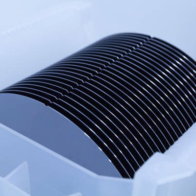
This 8 inch (200 mm) silicon carbide substrate is a prime grade 4H-N type wafer. It is engineered for power devices, RF modules, and heat-dissipation systems. The large size wafer helps manufacturing scale and lowers cost per device. It offers excellent thermal, electrical, and mechanical performance.
Key Features
High Thermal Conductivity
Silicon carbide offers much higher heat transfer than traditional silicon.
This allows better cooling and more reliable operation in hot environments.
High Breakdown Field Strength
The 4H-SiC substrate can handle high voltages and strong electric fields.
It supports devices with high power density and demanding specifications.
Wide Bandgap Performance
With a wide bandgap, the material sustains high temperature and high frequency use.
This makes it suitable for next-generation electronics and harsh environments.
Large Diameter Efficiency
The 8-inch (200 mm) size enables more devices per wafer.
It boosts production yield and supports cost-effective scaling.
Low Defect Density and Robust Quality
Manufactured with strict control of micropipes, bow, warp, and thickness.
This ensures consistent performance of downstream devices.
Applications
-
Power electronics: MOSFETs, diodes, converters for EVs and industrial systems.
-
RF devices: Amplifiers, 5G modules, high-frequency systems.
-
Heat dissipation modules: Systems where thermal management is critical.
-
Renewable energy: Inverters, smart grid components, energy storage systems.
-
Aerospace & defense: High temperature and high reliability electronics.
-
Research & development: Wide bandgap semiconductor platforms and prototyping.
Customization & Support
We offer customization options such as alternate thickness, orientation, and surface polish.
Surfaces can be polished or CMP finished for epitaxial growth.
We supply full documentation and support for integration into your device process.
Logistics and packaging are designed for safe delivery globally.
Why Choose This Substrate
Choosing this 8-inch SiC substrate means you select a wafer built for demanding performance.
The large size reduces cost per device and increases throughput.
The material’s superior thermal and electrical properties support efficient, reliable devices.
It is a future-proof foundation for power electronics, RF modules, and advanced semiconductor systems.


评价
目前还没有评价